Maxim¹«Ë¾µÄMAX98357A/MAX98357BÊÇÊý×ÖÂöÂëµ÷ÖÆ(PCM)ÊäÈëDÀà·Å´óÆ÷,ÌṩABÀàÒôƵÐÔÄܺÍDÀàЧÂÊ,ÓÐÎå¸ö¿ÉÑ¡ÔñµÄÔöÒæÉ趨(3dB, 6dB, 9dB, 12dBºÍ15dB),µ¥µçÔ´2.5V-5.5V¹¤×÷,5V 4¦¸Ê±µÄÊä³ö¹¦ÂÊΪ3.2W,ЧÂÊ92% (RL = 8¦¸, POUT = 1W),Êä³öÔëÒô25¦ÌVRMS (AV = 15dB),1kHzʱµÄTHD+NΪ0.015%,Ö÷ÒªÓÃÔڱʼDZ¾µçÄÔºÍÉÏÍø±¾(Netbook),ÊÖ»úºÍƽ°åµçÄÔ.±¾ÎĽéÉÜÁËMAX98357A/MAX98357BÖ÷ÒªÌØÐÔ,¹¦ÄÜ¿òͼºÍ¼¸ÖÖÓ¦Óõç·,ÒÔ¼°MAX98357¿ª·¢°åDEV(WLP)Ö÷ÒªÌØÐÔ,¿òͼ,µç·ͼ,²ÄÁÏÇåµ¥ºÍPCBÉè¼Æͼ.
The MAX98357A/MAX98357B are digital pulse-code mod-ulation (PCM) input Class D power amplifiers that provide Class AB audio performance with Class D efficiency. These ICs offer five selectable gain settings (3dB, 6dB, 9dB, 12dB, and 15dB) in I2S/left-justified mode set by a single gain select input and a fixed 12dB gain in TDM mode.
The digital audio interface is highly flexible with the MAX98357A supporting I2S data and the MAX98357B supporting left-justified data. Both ICs support 8 channel time division multiplexed (TDM) data. The digital audio interface accepts specified sample rates between 8kHz and 96kHz for all supported data formats. The ICs can be configured to produce a left channel, right channel, or (left/2 + right/2) output from the stereo input data. The ICs operate using 16/24/32-bit data for I2S and left-justified modes as well as 16-bit or 32-bit data using TDM mode. The ICs eliminate the need for the external MCLK signal that is typically used for PCM communication. This reduc-es EMI and possible board coupling issues in addition to reducing the size and pin count of the ICs.
The ICs also feature a very high wideband jitter toler-ance (12ns typ) on BCLK and LRCLK to provide robust operation.Active emissions-limiting, edge-rate limiting, and over-shoot control circuitry greatly reduce EMI. A filterless spread-spectrum modulation scheme eliminates the need for output filtering found in traditional Class D devices and reduces the component count of the solution.
The ICs are available in 9-pin WLP (1.345mm x 1.435mm x 0.64mm) and 16-pin TQFN (3mm x 3mm x 0.75mm) packages and are specified over the -40 ¡æ to +85¡æ tem-perature range.
MAX98357A/MAX98357BÖ÷ÒªÌØÐÔ:
Single-Supply Operation (2.5V to 5.5V)
3.2W Output Power into 4¦¸ at 5V
2.4mA Quiescent Current
92% Efficiency (RL = 8¦¸, POUT = 1W)
25¦ÌVRMS Output Noise (AV = 15dB)
Low 0.015% THD+N at 1kHz
No MCLK Required
Sample Rates of 8kHz to 96kHz
Supports Left, Right, or (Left/2 + Right/2) Output
Sophisticated Edge Rate Control Enables Filterless Class D Outputs
77dB PSRR at 1kHz
Low RF Susceptibility Rejects TDMA Noise from GSM Radios
Extensive Click-and-Pop Reduction Circuitry
Robust Short-Circuit and Thermal Protection
Available in Space-Saving Packages: 1.345mm x 1.435mm WLP (0.4mm Pitch) and 3mm x 3mm TQFN
MAX98357A/MAX98357BÓ¦ÓÃ:
Notebook and Netbook Computers
Cellular Phones
Tablets

ͼ1.MAX98357A/MAX98357B¹¦ÄÜ¿òͼ

ͼ2.MAX98357A/MAX98357BÔöÒæ6dB×ó·PCM¹¤×÷µç·
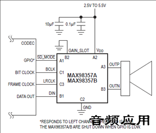
ͼ3.MAX98357A/MAX98357BÔöÒæ12dB×ó·PCM¹¤×÷µç·

ͼ4.MAX98357A/MAX98357BÔöÒæ6dBÓÒ·PCM¹¤×÷µç·

ͼ5.MAX98357A/MAX98357BÔöÒæ6dB(×ó·/2+ÓÒ·/2)PCM¹¤×÷µç·

ͼ6.MAX98357A/MAX98357B²ÉÓÃÁ½¸öICµÄÁ¢ÌåÉùPCM¹¤×÷µç·

ͼ7.MAX98357A/MAX98357BÔöÒæ12dBͨ·TDM¹¤×÷µç·
|


 »Ø¸´